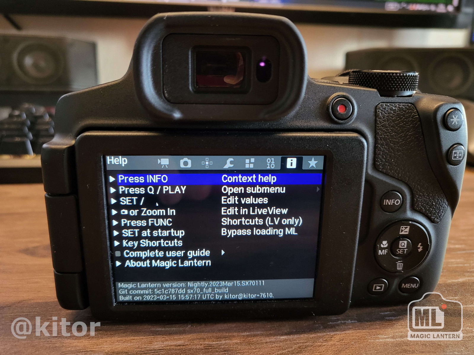
Turns out that "Powershot" based models don't have MPU but use small Cortex M0 instead. At least on SX70 and SX740, I don't have a good photo of M50 to confirm.
But there seems to be a visually matching chip, SD slot side, bottom right corner if SD slot is facing down.
M17M6, 36 pin XFBGA -> https://www.nxp.com/docs/en/data-sheet/KL17P64M48SF2.pdf
Today I desoldered DIGIC and that Cortex M0 from my water damaged SX70 HS board.
https://twitter.com/_kitor/status/1656369031383773188
With some measurements I was able to identify about 1/2 of the pins.
It doesn't seem to have any UART output.
Interesting ones: Power, Play and WiFi buttons go to Cortex M0, not ICU. This makes sense as both can wake up the camera.
However INFO button also goes to M0. Reason is unknown.
Code Select
pin  where?         signal    (mode)
A1
A2
A3
A4  to DIGIC        SPI0_MISO (alt2)
A5  to DIGIC        SPI0_SCLK (alt2)
A6  to DIGIC        SPI0_PCS0 (alt2)
B1
B2
B3
B4  to DIGIC        SPI0_MOSI (alt2)
B5
B6
C1
C2  button Play     PTE16     (alt1)
C3                  VDD
C4                  GND
C5
C6  at DNE chip     I2C0_SDA  (alt2)
D1
D2
D3  VDDA
D4  GND
D5  at debug conn   RESET     (default)
D6  at DNE chip     I2C0_SCL  (alt2)
E1
E2
E3
E4  button Power    PTA2      (alt1)
E5  at debug conn   SWD_IO    (default)
E6  at crystal      EXTAL_0   (default)
F1  button INFO     PTE23     (alt1)
F2
F3  at debug conn   SWD_CLK   (default)
F4  button WIFI     PTA1      (alt1)
F5
F6  at crystal      XTAL_0    (default)  @crystal


 :
: